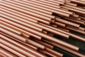
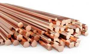
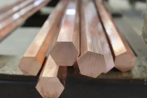
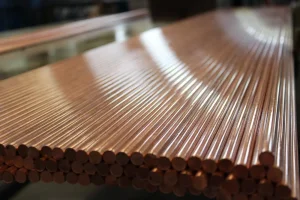
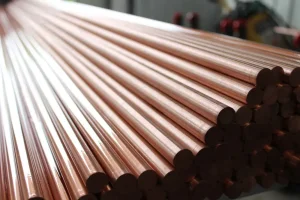
In the landscape of modern industrial metallurgy, CW113C (also known as CuPb1P) represents a critical balance between high electrical conductivity and superior machinability. As global manufacturing pivots toward high-speed precision machining, the demand for leaded copper alloys that do not compromise on electrical performance has surged.
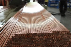
The copper alloy market is currently driven by the EV (Electric Vehicle) revolution and the expansion of 5G infrastructure. CW113C, characterized by its inclusion of lead for chip-breaking, allows for complex geometric manufacturing at high speeds. Unlike pure copper, which is notorious for being "gummy" and difficult to machine, CW113C provides an efficient solution for connectors, switches, and complex electronic components.
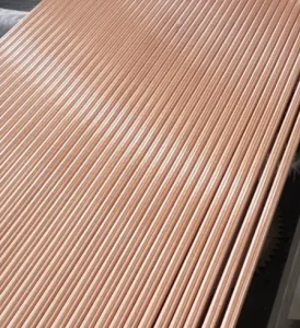
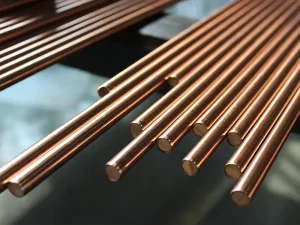
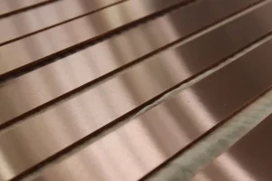
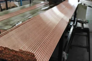
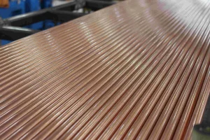
Sichuan Kepai New Materials Co., Ltd. emphasizes the molecular-level integrity of CW113C. By controlling the distribution of lead particles within the copper matrix, we ensure that:
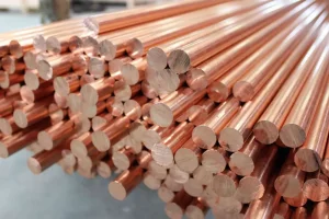
While the industry trends toward lead-free materials, for specific high-performance applications where thermal dissipation and conductivity are paramount, CW113C remains an irreplaceable standard. Our R&D team is currently exploring "Green Machining" techniques to further optimize the utilization of leaded alloys, ensuring compliance with global environmental standards while maximizing output efficiency.
Established in 2017, we are a high-tech enterprise integrating research, development, and production. Our 9,000 sqm facility is at the forefront of the national 13th Five-Year Plan for strategic new materials.
Our core competitiveness lies in our expert R&D team. We specialize in high-performance copper alloys, bridging the gap between basic raw materials and high-end industrial applications such as laser cutting, new energy vehicles, and 5G signal relays.
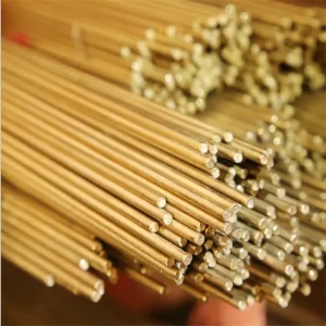
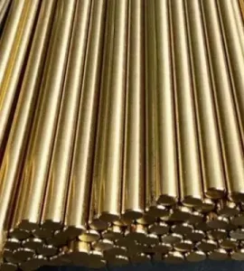
A: CW113C offers the optimal combination of electrical conductivity and "free-cutting" capabilities. If your production line requires high-speed CNC machining for complex electrical parts, CW113C reduces tool wear and increases throughput.
A: We utilize advanced spectroscopy and eddy current testing to ensure uniform distribution of alloy elements, adhering to strict international standards.